- 您现在的位置:买卖IC网 > Sheet目录1991 > CS5509-ASZR (Cirrus Logic Inc)IC ADC 16BIT SGL SUPP 16-SOIC
CS5509
DS125F3
9
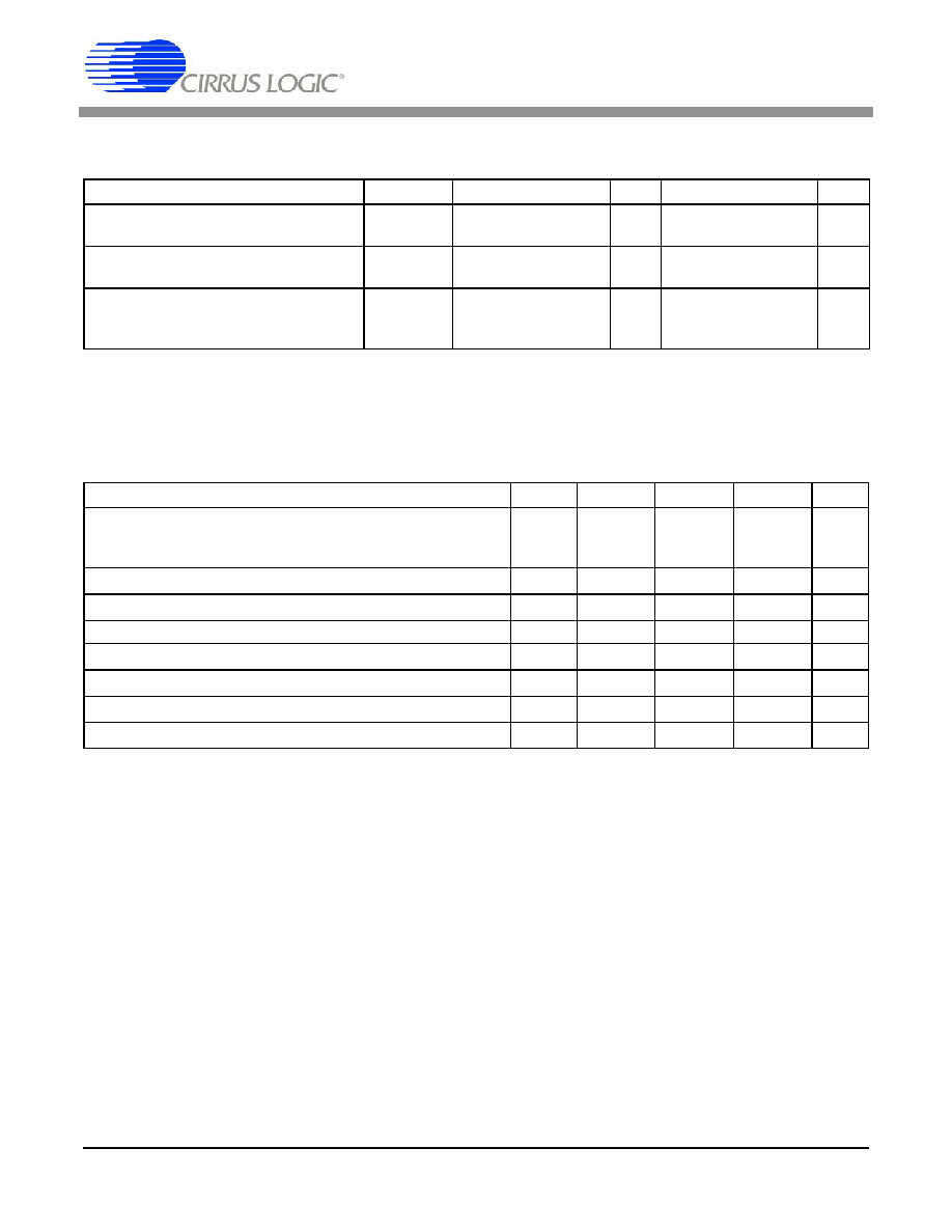
Notes: 19. All voltages with respect to ground.
20. The CS5509 can be operated with a reference voltage as low as 100 mV; but with a corresponding
reduction in noise-free resolution. The common mode voltage of the voltage reference may be any value
as long as +VREF and -VREF remain inside the supply values of VA+ and GND.
Notes: 21. No pin should go more positive than (VA+) + 0.3 V.
22. VD+ must always be less than (VA+) + 0.3 V, and can never exceed +6.0 V.
23. Applies to all pins including continuous overvoltage conditions at the analog input (AIN) pin.
24. Transient currents of up to 100 mA will not cause SCR latch-up. Maximum input current for a power
supply pin is ± 50 mA.
25. Total power dissipation, including all input currents and output currents.
*WARNING:Operation at or beyond these limits may result in permanent damage to the device.
Normal operation is not guaranteed at these extremes.
RECOMMENDED OPERATING CONDITIONS (DGND = 0V) (Note 19)
Parameter
Symbol
Min
Typ
Max
Unit
DC Power Supplies
Positive Digital
Positive Analog
VD+
VA+
3.15
4.75
5.0
5.5
V
Analog Reference Voltage
(Note 20)
(VREF+) -
(VREF-)
1.0
2.5
3.6
V
Analog Input Voltage
(Note 6)
Unipolar
Bipolar
VAIN
0
-((VREF+) - (VREF-))
-
(VREF+) - (VREF-)
V
ABSOLUTE MAXIMUM RATINGS*
Parameter
Symbol
Min
Typ
Max
Unit
DC Power Supplies
Ground
(Note 21)
Positive Digital
(Note 22)
Positive Analog
GND
VD+
VA+
-0.3
-
(VD+)-0.3
6.0
V
Input Current, Any Pin Except Supplies
Iin
--
±10
mA
Output Current
Iout
--
±25
mA
Power Dissipation (Total)
(Note 25)
-
500
mW
Analog Input Voltage
AIN and VREF pins
VINA
-0.3
-
(VA+)+0.3
V
Digital Input Voltage
VIND
-0.3
-
(VD+)+0.3
V
Ambient Operating Temperature
TA
-40
-
85
°C
Storage Temperature
Tstg
-65
-
150
°C
发布紧急采购,3分钟左右您将得到回复。
相关PDF资料
CS5512-BSZ
IC ADC 20BIT EXTERNAL OSC 8-SOIC
CS5526-BSZR
IC ADC 20BIT W/4BIT LATCH 20SSOP
CS5528-ASZR
IC ADC 24BIT 8CH 24-SSOP
CS5529-ASZR
IC ADC 16BIT W/6BIT LATCH 20SSOP
CS5530-ISZR
IC ADC 24BIT 1CH W/LNA 20-SSOP
CS5534-ASZR
IC ADC 24BIT 4CH W/LNA 24-SSOP
CS5534-BSZR
IC ADC 24BIT 4CH W/LNA 24SSOP
CS5550-ISZR
IC ADC 2CH LOW-COST 24-SSOP
相关代理商/技术参数
CS5510
制造商:CIRRUS 制造商全称:Cirrus Logic 功能描述:16-bit and 20-bit, 8-pin ΔΣ ADCs
CS5510_09
制造商:CIRRUS 制造商全称:Cirrus Logic 功能描述:16-bit and 20-bit, 8-pin ΔΣ ADCs
CS5510-AS
功能描述:模数转换器 - ADC 16-Bit Delta Sigma ADC Ext. OSC RoHS:否 制造商:Texas Instruments 通道数量:2 结构:Sigma-Delta 转换速率:125 SPs to 8 KSPs 分辨率:24 bit 输入类型:Differential 信噪比:107 dB 接口类型:SPI 工作电源电压:1.7 V to 3.6 V, 2.7 V to 5.25 V 最大工作温度:+ 85 C 安装风格:SMD/SMT 封装 / 箱体:VQFN-32
CS5510-ASR
功能描述:模数转换器 - ADC IC 16-Bit 8-Pin Delta Sigma ADC RoHS:否 制造商:Texas Instruments 通道数量:2 结构:Sigma-Delta 转换速率:125 SPs to 8 KSPs 分辨率:24 bit 输入类型:Differential 信噪比:107 dB 接口类型:SPI 工作电源电压:1.7 V to 3.6 V, 2.7 V to 5.25 V 最大工作温度:+ 85 C 安装风格:SMD/SMT 封装 / 箱体:VQFN-32
CS5510-ASZ
功能描述:模数转换器 - ADC 16-Bit Delta Sigma ADC Ext. OSC RoHS:否 制造商:Texas Instruments 通道数量:2 结构:Sigma-Delta 转换速率:125 SPs to 8 KSPs 分辨率:24 bit 输入类型:Differential 信噪比:107 dB 接口类型:SPI 工作电源电压:1.7 V to 3.6 V, 2.7 V to 5.25 V 最大工作温度:+ 85 C 安装风格:SMD/SMT 封装 / 箱体:VQFN-32
CS5510-ASZ
制造商:Cirrus Logic 功能描述:A/D Converter (A-D) IC
CS5510-ASZR
功能描述:模数转换器 - ADC IC 16-Bit 8-Pin Delta Sigma ADC RoHS:否 制造商:Texas Instruments 通道数量:2 结构:Sigma-Delta 转换速率:125 SPs to 8 KSPs 分辨率:24 bit 输入类型:Differential 信噪比:107 dB 接口类型:SPI 工作电源电压:1.7 V to 3.6 V, 2.7 V to 5.25 V 最大工作温度:+ 85 C 安装风格:SMD/SMT 封装 / 箱体:VQFN-32
CS5511
制造商:CIRRUS 制造商全称:Cirrus Logic 功能描述:16-bit and 20-bit, 8-pin ΔΣ ADCs